Product Detail
Share to:

TMGG13228

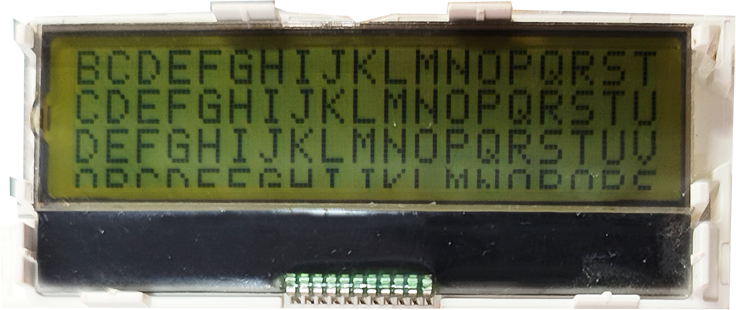
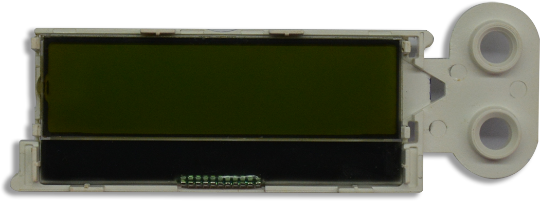
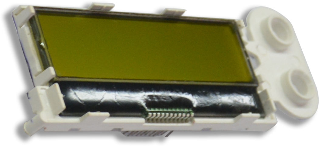
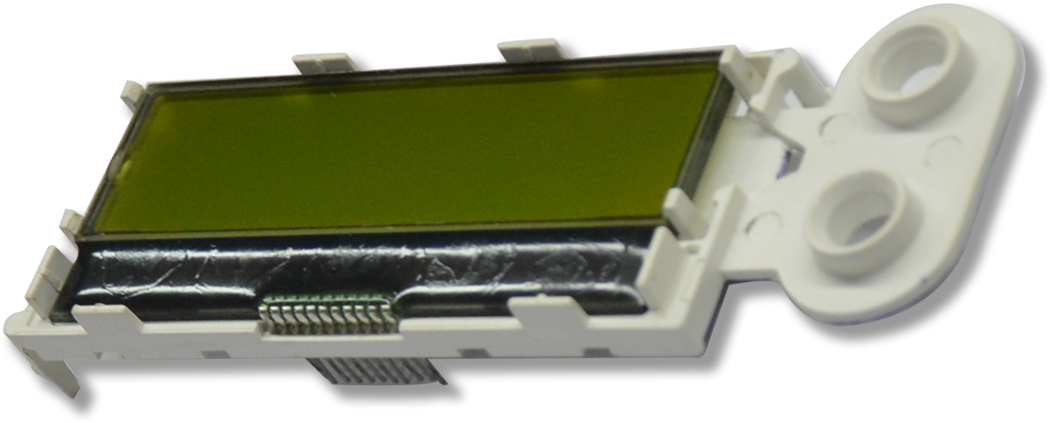
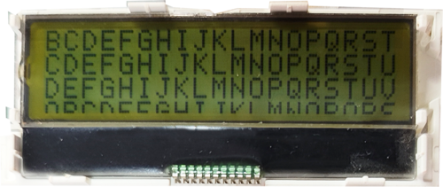
Format: 132 * 28 dots
LCD Mode: STN, Positive, Yellow-Green, Transflective
Viewing Direction: 6 o'clock
Driving Scheme: 1/33 Duty cycle, 1/6 Bias
Single Supply Voltage: Power supply voltage range (VDD): 2.4~3.6V
Low current sleep mode
64 levels of Internal Contrast Control  
4-line Serial Interface
Scrolling function
On-Chip Oscillator Circuit
On-Chip voltage regulator and voltage follower
Display Offset Control
On-chip DC-DC Converter
RoHS Compliance
With Plastic Mount
Product Details
Interface
Mechanical Spec.
Full Spec.
Resolution 132 * 28 Dots Module Size (mm) 62.00 * 28.50
Viewing Area (mm) 58.00 * 15.00 Character Size/Dot Pitch (mm) 0.416 * 0.468
Dot Size (mm) 0.386 * 0.438 Type COG
Connection Metal Pin IC SSD1838 or equivalence
Display Mode +Ve or -Ve/ STN, FSTN, FFSTN Backlight Color YG, R, G, B, W

Pin no.

Symbol

Function

1

ESD-GND

Electro-static discharge protection ground, 0V

2

/CS

Chip select pin. Chip is selected when /CS=L.

3

/RES

This pin is the reset signal input. Initialization ofthe chip is started once this pin is pulled low.

Minimum pulse width for reset sequence is 20us.

4

D/C

This pin is Data/Command control pin. When thepin is pulled high, the data at D7 - D0 is treated asdisplay data. When the pin is pulled low, the data

at D7 - D0 will be transferred to the commandregister.

5

SCK

Serial clock input pin

6

SDA

Serial data input pin

7

VSS

Power supply, 0V

8

VDD

Power supply, +3.0V

9

VOUT

This is the most positive voltage supply pin of thechip. It is output of internal DC-DC converter. Connect a capacitor between this pin and VSS.

10

V0

Power supply for LCD driver. Connect a capacitor between this pin and VSS.

11

ESD-GND

Electro-static discharge protection ground, 0V


TMGG13228-04-CDA03.pdf


TMGG13228-04-SPA01.pdf


Sustainability
website qrcode
Head Office: Unit A, 6/F, Houtex Industrial Building, 16 Hung To Road, Kwun Tong, Kowloon, Hong Kong, China
Tel: (852) 2342 1136 E-mail:sales@3-t.com.hk