Chip select pin. Chip is selected when CS0=L. When chip is not selected, D[0:7] will be in high impedance.
2
/RST
External reset pin, low active. If RST not used, connect to VDD
3
CD
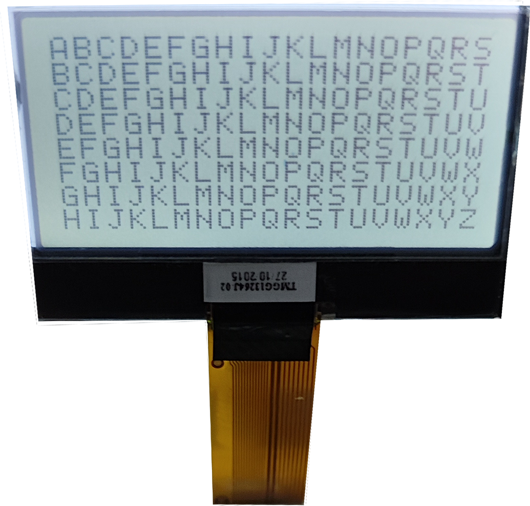
Display/control data select “H”:display data ; “L”:control data
4
WR0
WR [1:0] controls the read/write operation of the host interface.In parallel mode, the meaning of WR[1:0] depends on which interface it is in, 6800 or 8080 mode. In serial interface modes, these two pins are not used, Connect them to VSS or VDD.
5
WR1
6
D0
Bi-directional bus for both serial and parallel host interfaces.In serial modes, connect D[7] to SDA, D[6] to SCK.In serial modes, Always connect unused pins to either VSS or VDD.
7
D1
8
D2
9
D3
10
D4
11
D5
12
D6
13
D7
14
VDD
Power supply, +3.0V.
15
VSS
Power supply, 0V.
16
VB0-
LCD bias voltage is generated internally. Connect 1uF capacitors between VB0+ and VB0-.
17
VB0-
18
VB1-
LCD bias voltage is generated internally. Connect 1uF capacitors between VB1-and VB1+.
19
VB1+
20
VLCD
Internal DC/DC converter output voltage pin. Connect a 1uF capacitor between this pin and VSS for voltage de-coupling
21
BM0
Bus mode: The interface bus mode is determined by BM[1:0] and {D7, D6} by the following relationship:BM=1x (8-bit),{D7, D6}(Data)/ BM=0x (S8){D7, D6},(SDA, SCK);