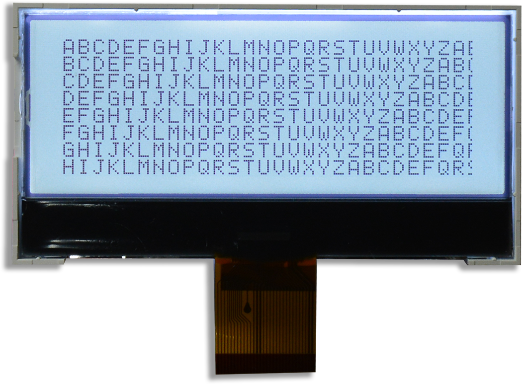
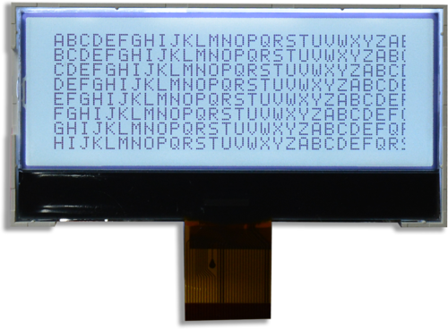
Format: 192 * 64 dots LCD Mode: STN, Negative/Blue/Transmissive Mode Viewing Direction: 12 o'clock Driving Scheme: 1/65 Duty cycle, 1/9 Bias Single Supply Voltage: Power supply voltage range (VDD): 2.7~3.6V Backlight Color: White 64 level of Internal Contrast Control 68 or 80 series parallel interface, Serial Interface Scrolling function On-chip DC-DC Converter RoHS Compliance
-Serial-mode, (PS = “L”), C86 must be fixed to “H” or “L”.
29
V4
LCD driver supply voltages
The voltage determined by LCD pixel is impedance- converted by an operational
amplifier for application.
Voltages should have the following relationship;
V0 ≥ V1 ≥ V2 ≥ V3 ≥ V4 ≥ VSS
When the internal power circuit is active, these voltages are generated as following as
following table according to the state of LCD bias.
LCD Bias
V1
V2
V
V4
1/9 bias
(8/9)* V0
(7/9)* V0
(2/9)* V0
(1/9)* V0
28
V3
27
V2
26
V1
25
V0
24
C2-
LCD bias voltage are generated internally. Connect a 1uF capacitors between C1+ and C1-, C2+ and C2-, C1- and C3+
23
C2+
22
C1+
21
C1-
20
C3+
19
VOUT
Internal DC/DC converter output pin, need to connect a 1uF capacitor between VSS and this pin for voltage decoupling
18
VSS2
Power supply, 0V .
17
VDD2
Power supply, +3.3V.
16
PS
Parallel / serial data input select input
15 ~ 8
D7 ~ D0
8-bit bi-directional data bus that is connected to the standard 8-bit microprocessor data bus. When the serial interface selected (PS = “L”); -DB0 to DB5 : Keep VDD or VSS
- DB6 : serial input clock (SCLK)
- DB7 : serial input data (SID)
When chip select is not active, DB0 to DB7 may be high impedance.
7
RDB
Read / Write execution control pin
H
6800-series
E
Read / Write control input pin
- RW = “H” : When E is “H”, DB0 to DB7 are in an output status.
- RW = “L” : The data on DB0 to DB7 are latched at the falling edge the E signal.
L
8080-series
RD
Read enable clock input pin
When / RDB is “L”, DB0 to DB7 are in an output status.
6
WRB
Read / Write execution control pin
H
6800-series
RW
Read / Write control input pin
- RW = “H” : read ; /- RW = “L” : write
L
8080-series
WR
Write enable clock input pin
The data on DB0 to DB7 are latched at the rising edge of the WRB signal.
5
A0
Display/control data select “H”:display data; “L”:control data
4
/RESB
Reset input pin When /RES is “L”, initialization is executed.
3
/CS1B
Chip select input pins
Data / instruction I/O is enabled only when CS1B is “L” and CS2 is “H”. when chip
select is non-active, DB0 to DB7 may be high impedance.
2
VDD1
Power supply, +3.3V.
1
VSS1
Power supply, 0V.
Backlight Pins:
BL 1
A(LED+)
Anode of LED backlight (+3.3V, LEDs in parallel connection)