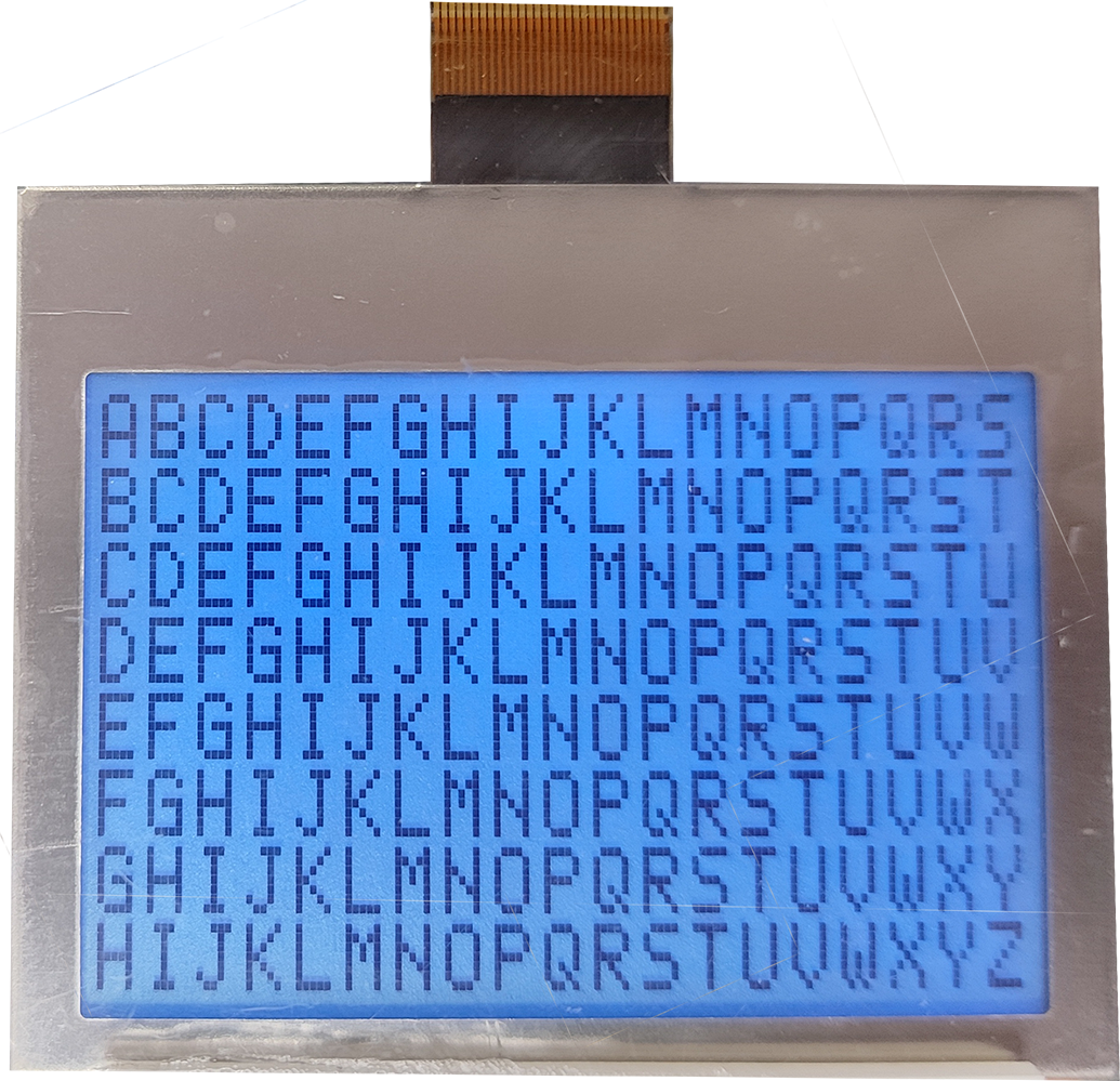
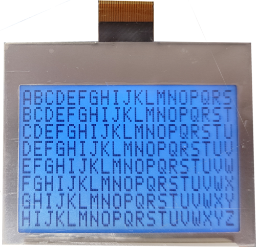
Format: 132 * 64 dots LCD Mode: FSTN/ Positive/B&W/Transflective Mode Viewing Direction: 6 o'clock Driving Scheme: 1/65 Duty cycle, 1/9 Bias Single Supply Voltage: Power supply voltage range (VDD): 2.7~3.5V Low current sleep mode 64 level of Internal Contrast Control and External Contrast Control Parallel or Serial Interface Vertical Scrolling, Display offset control and RAM Page blinking On-chip DC-DC Converter
“H” :for using internal resistor network to generate LCD driving voltage. “L” for using external resistors, two resistors R1/R2 should be connected between VDD & VF and VF & VL6.
2
P/S
Parallel or Serial Interface. “H”: Parallel; ”L” Serial
3
C68
Select I/O“H”:6800 series; “L”:8080 series
4
VR
Output voltage regulator terminal. Provides the voltage between VSS and V0 through a
resistive voltage divider.
IRS = L: the V0 voltage regulator internal resistors are not used.
IRS = H: the V0 voltage regulator internal resistors are used.
5
V0
LCD driving voltage
1).VDD>V0>V1>V2>V3>V4
2).V1=8/9V0,V2=7/9V0,V3=2/9V0,V4=1/9V0
Connect 1uF capacitors between these voltages & VSS
6
V1
7
V2
8
V3
9
V4
10
C2N
Charge pump capacitors connecting terminals
11
C2P
12
C1P
13
C1N
14
C3P
15
VOUT
DC/DC voltage converter. Connect a capacitor between this terminal and VSS or VDDterminal.