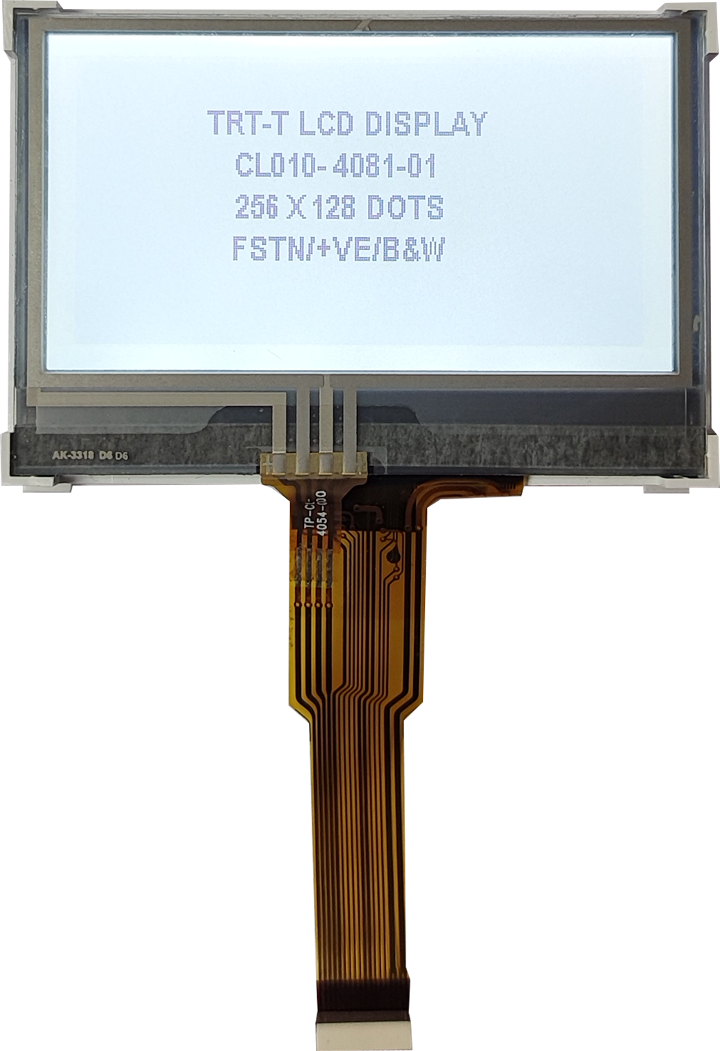
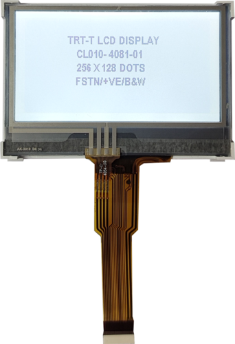
Pin no.
Symbol
Function
1~4
NC
No connection.
5
VLCD
Voltage level for LCD driving
6~9
VB0+,VB0-VB1-,VB1+
LCD Bias Voltages. These are the voltage sources to provide SEG driving currents. These voltages are generated internally.
10
VSS
Power supply (0V)
11
VDD
Power supply (0V) Power supply (+2.7 ~ +3.6V)
12
SDA
I2C data signal input pin
13
SCL
I2C clock signal input pin
14
RST
Hardware reset input pin. When RSTB is "L", internal initialization is executed and theinternal registers will be initialized.
15~18