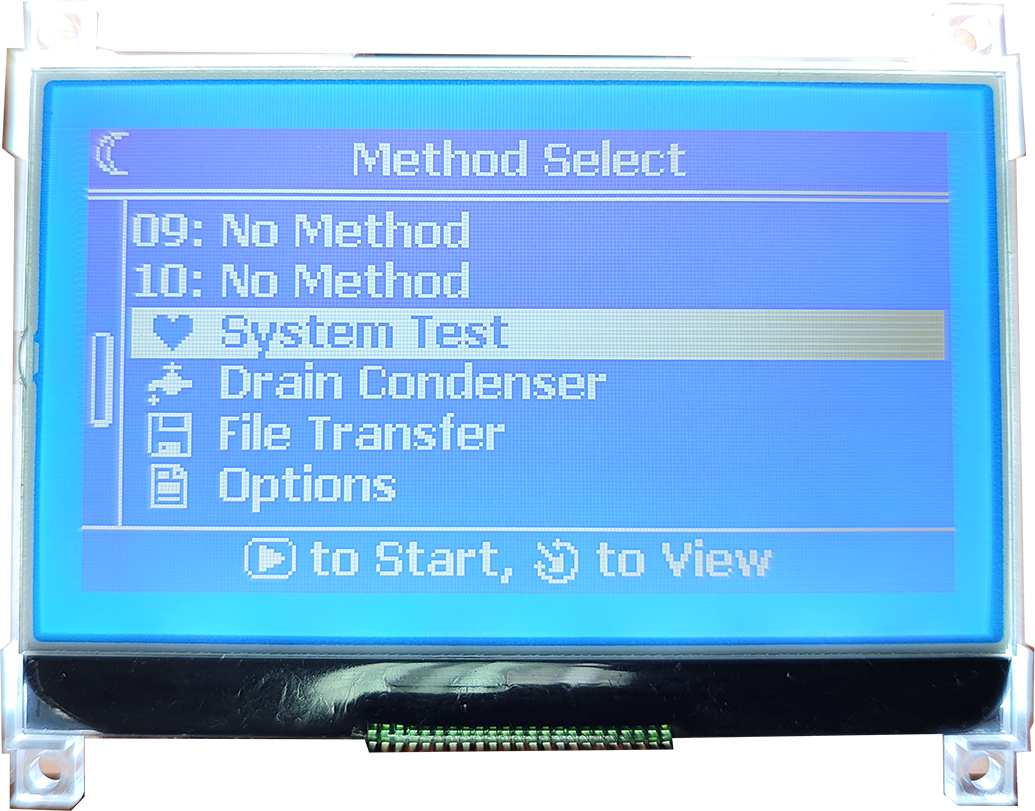
LCD bias voltage are generated internally. Connect a 0.1uF ~1uF capacitors between VB1+ and VB1-, VB0+ and VB0-.
2
VB1+
3
VB0-
4
VB0+
5
VLCD
Internal DC/DC converter output pin, need to connect a 4.7uF capacitor between VSS and this pin for voltage decoupling
6
VBAIS
This is the reference voltage to generate the actual SEG driving voltage. VBIAS can be used to fine tune VLCD by external variable resistors. Internal resistor network has been provided to simplify external trimming circuit. Connect a small bypass capacitor between VBIAS and VSS
7
VSS
Power supply, 0V
8
VDD
Power supply, +3.0V
9
D7
Bi-directional bus for both serial and parallel interfaces. In serial mode, connect D[0] to SCK, D[3] to SDA.
BM=1X
(8 bit)
BM=00
(S8)
BM=01
(S9)
BM=00
(I2C)
D0
D0
SCK
SCK
SCK
D1
D1
--
--
--
D2
D2
--
--
--
D3
D3
SDA
SDA
SDA
D4
D4
--
--
--
D5
D5
--
--
--
D6
D6
0
0
1
D7
D7
1
1
1
Unused pins should be connected to VSS or VDD
10
D6
11
D5
12
D4
13
D3
14
D2
15
D1
16
D0
17
WR1
In serial mode, these pins are not used, connect to VSS. In parallel mode, functions as following table:
I/O type
(8080 I/O)
(6800 I/O)
WR0
/WR
R/W
WR1
/RD
E
18
WR0
19
CD
Display/control data select “H”:display data; “L”:control data. In S9 mode connect CD to Vss
20
RST
External reset pin, low active. If RST not used, connect to VDD
21
CS
Chip select pin. Chip is selected when CS=H. When chip is not selected, D[7:0] is high impedance.
22
BM0
Bus mode: The interface bus mode is determined by BM[1:0] and {DB7,DB6} by the following relationship :
BM[1:0]
{DB7, DB6}
Mode
11
Data
6800/8 bit
10
Data
8080/8 bit
01
0X
6800/4 bit
00
0X
8080/4 bit
01
10
3-wire SPI w/9-bit token(S9:conventional)
00
10
4-wireSPI w/8-bit token (S8:conventional)
01
11
3 / 4 wire SPI w/8-bit token
(S8uc:Ultra-Copmact)
23
BM1
A
A(LED+)
Anode of LED backlight (+3.3V, LEDs in parallel connection)