Pin no.
Symbol
Function
1
SCK
Serial clock input pin
2
SDA
Serial data input pin
3
/RST
External reset pin, low active
4
/CS
Chip select pin, low active
5
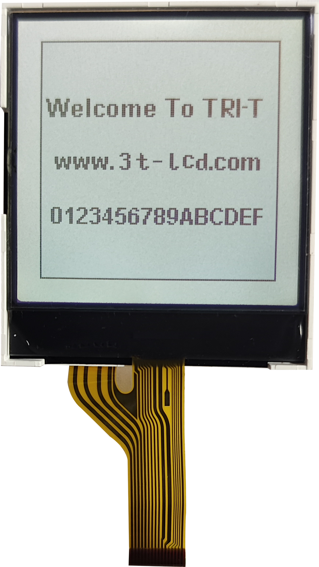
C/D
Select control or display data signal, H=display data; L=control data
6
VSS
Power supply, 0V
7
VDD
Power supply, +3.3V
8
VB0+
LCD bias voltage are generated internally. Connect a 2.2uF capacitors between VB0+ and VB0-, VB1+ and VB1-.
9
VB1+
10
VB1-
11
VB0-
12
VLCD
Internal DC/DC converter output pin, need to connect a 330nF ~ 1uF capacitor between VSS and this pin for voltage decoupling.
13
NC
No connection
14
K2
Cathode of LED2
15
K1
Cathode of LED1
16
A
Command anode of the LED backlight