Pin no.
Symbol
Function
1
FG
Frame ground
2
VSS
Power supply (0V)
3
VDD
Power supply (+3.3V)
4
V0
VLCD driving voltage input. When using internal DC/DC converter and temperature compensation circuit, leave this pin open.
5
/WR
Data Write (write data into LCM when /WR=L)
6
/RD
Data Read (read data from LCM when /RD=L)
7
/CE
Chip enable for LCM
8
C/D
Control read (H=status; L=data) and
write (H=command; L=data)
9
VEE
Internal DC/DC converter voltage output (-10V)
10
/RST
Reset, low active
11~18
DB0 ~ DB7
Data Bus
19
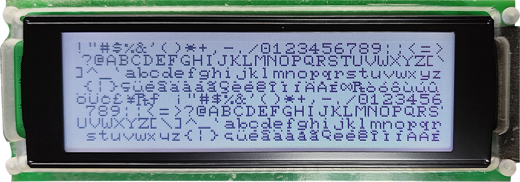
FS
Select font (H=6*8; L=8*8)
20
PD
Power Down select: H=Normal operation, L =Power Down.
Internal pull high.
A
LED+
Anode input for LED backlight
K
LED-
Cathode input for LED backlight