Pin no.
Symbol
Function
1
VDD
Supply voltage for logic circuit (+5V)
VSS
Ground
3
V0
NC (LCD driving voltage, internally generated and temperature compensated)
4
DB0
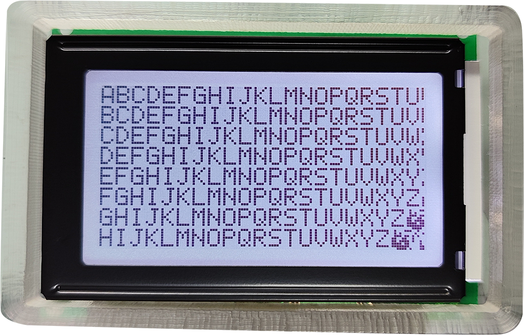
Display data signal
5
DB1
6
DB2
7
DB3
8
DB4
9
DB5
10
DB6
11
DB7
12
CS1
Chip select for driver 1 (Segment 0~63), high active
13
CS2
Chip select for driver 2 (Segment 64~127), high active
14
RESET
External reset, low active
15
R/W
Use as read/ write select input
16
D/I
Selects register data“H”or instruction“L”
17
E
Use as read/ write enable input
18
FGND
Frame ground
19
LED+
LED Backlight Anode
20
LED -
LED Backlight Cathode